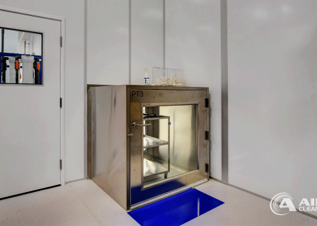
Semiconductor Cleanrooms
Just imagine your wafer fab line shutting down from a stray 0.1-micron particle. Millions in scrap silicon, missed chip launches, and competitors taking your share of AI or 5G markets. At the dawn of sub-10nm nodes, what if your cleanroom blocked 99.999% of particles and held temperature swings within ±1°F for precise photolithography?
Semiconductor cleanrooms aren’t a luxury; they’re the ironclad defense against particles that torch wafer yields. A single mote of dust in photolithography can cause defects, spike scrap rates, and bleed margins. Ultra-controlled ISO 4–5 environments block microbes and submicron particles, shielding every 0.1-micron line from failure. Without them, fabs grind to a halt under FED STD 209E violations, losing $10K for every downtime hour. The result? Solid cleanrooms deliver repeatable 90%+ yields and faster ROI on your $500M toolset.
As nodes shrink, contamination control shifts from nice-to-have to do-or-die. Even a skin flake can ruin circuits, but controlled humidity at ±5% RH prevents photoresist warpage. Operators who ignore this see defect densities jump 50%, while smart fabs cut defects with real-time particle tracking. Cleanrooms aren’t just walls. They’re the fortress where wafer fabs protect their profits.
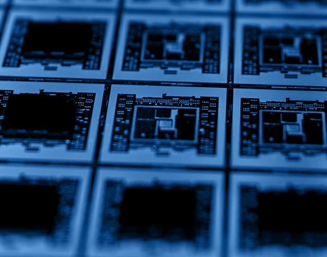
Form-Fitting Design for Flawless Fab Performance
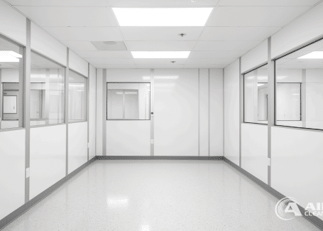
Full-ceiling ULPA filters create vertical laminar flow, capturing 99.999% of 0.12µm particles before they strike photolithography bays. Amber lighting prevents UV degradation, raised floors streamline air returns, and static-dissipative vinyl eliminates ESD spikes. These measures drive air changes every 10 seconds, cutting viable counts to near zero and boosting throughput by 15%.
Dedicated HVAC systems hold temps at ±1°F and humidity within ±5–10% RH, protecting against thermal drift. Operators enter through air showers and glove ports, shedding 99% of contaminants before touching the line. Real-time dashboards detect surges, giving engineers control before failures cascade. Fabs running this design save 25% on energy while maintaining airtight process control.
From Pilot Fabs to Megafabs
From 500 sq. ft. R&D pods to 500,000 sq. ft. giants pushing 100K wafers a month, cleanrooms fuel every fab. Photolithography thrives under ISO 4 amber glows, etching ultra-fine masks free from haze-induced shorts. Deposition zones at ISO 5 stack layers with surgical precision, feeding etch processes that sculpt trillion-transistor wonders. Metrology at ISO 6–7 catches nanodefects before packaging, ensuring reliability.
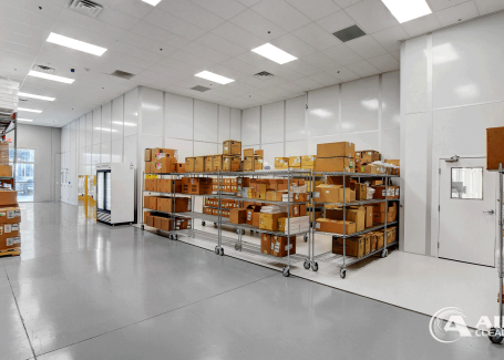
Backend assembly thrives under controlled ESD that protects bond pads from catastrophic craters. Pilot runs test next-gen nodes safely, while megafabs use utility chases for seamless DI water and N2 supply. Operators adopting these models cut cycle times by 30%, seizing leadership in EVs and quantum chips. Nail the fit, and your fab transforms from risky to unstoppable.
Cleanroom Classifications: ISO 4–7 in Semiconductor Fabs
ISO 4 (Class 10) governs photolithography and deposition, limiting particles to 10 per cubic foot at 0.5µm. ISO 5 (Class 100) manages etch bays with laminar sweeps to avoid turbulence traps. ISO 6 (Class 1,000) balances cost and control for metrology, while ISO 7 (Class 10,000) buffers packaging zones. Mismatch them, and yields crater 20%; align them, and fabs validate in weeks.
ISO 14644 sets the global standard, while SEMI adds vibration limits critical for EUV stability. Early audits save fabs from $100K retrofits and keep compliance airtight. These aren’t arbitrary boxes—they’re precision-tuned zones that protect processes from resist coating through singulation. Lock in the right classification, and your fab hums with audit-proof efficiency.
Modular Semiconductor Cleanrooms: Growth Muscle That Scales
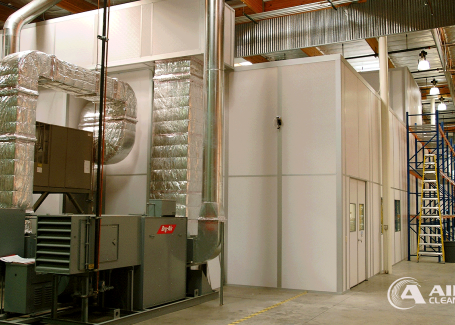
Modular builds bake in ISO 14644 and SEMI standards from day one, avoiding 6–12 month delays of custom builds. ULPA ceilings integrate with tools seamlessly, cutting install times by 50%. Smart insulation lowers HVAC loads by 20%, offsetting million-dollar annual bills in megafabs. From R&D to high-volume lines, modular setups deliver 99.9% uptime with built-in redundancy.
Custom sub-fabs minimize vibration bleed, protecting photolithography precision. Operators leveraging modular builds hit SEMI certification 40% faster, outflanking rivals in the chip wars. This isn’t flexibility, it’s a competitive advantage designed to survive Moore’s Law. Modular is the muscle that lets your fab scale without compromise.
Standards and Best Practices: ISO, FED STD, SEMI Compliance
ISO 14644 defines particle thresholds, while FED STD 209E remains for legacy fabs. SEMI standards amplify airflow, ESD control, and monitoring to meet the demands of advanced nodes. Non-compliance means expensive audits, paused shipments, and profit bleed. Build in viable sampling and ESD grounding from the start, and audits become a formality.
Automated monitoring logs halve validation cycles, freeing engineers to innovate instead of firefight. Compliance isn’t red tape—it’s fuel for global scale. Fabs leveraging these standards export confidently, bypassing tariff risks tied to non-conforming silicon. Done right, compliance becomes rocket fuel for market conquest.
Customization Options: How You Can Tailor Your Semiconductor Cleanrooms
Raised floors provide under-tool access and smooth airflow, while ESD-proof vinyl strengthens reliability. Amber shields fight UV-induced resist damage, and air showers lock contaminants at every entrance. Single-pass HVAC ensures ultra-pure airflow, while recirculating options maximize energy efficiency. Process chases streamline stepper feeds, turning dead zones into hidden assets.
Tailor every aspect to your fab’s footprint, and operations pivot from cost center to profit engine. Customization transforms your cleanroom from static infrastructure into a dynamic growth driver.
Precision Environments
Even small drifts wreck wafers. A 1°F swing or 5% RH shift can warp photoresist and throw nodes off. HVAC tuned tight, raised floors, and amber lights keep conditions steady. That stability holds photolithography, etch, and deposition in line and keeps throughput climbing instead of crashing.
Scalability
Stick-built fabs are slow and expensive. Modular cleanrooms install 50% faster, with insulation that lowers HVAC loads by 20%. From pilot fabs to megafabs, modular design allows expansion, relocation, or reconfiguration without halting operations, keeping pace with Moore’s Law and enabling fabs to scale without compromise.
Compliance Built In
Fabs run on standards such as ISO 14644, SEMI, and older FED STD 209E. Build to spec and inspections move faster, with smoother validation and easier market access.
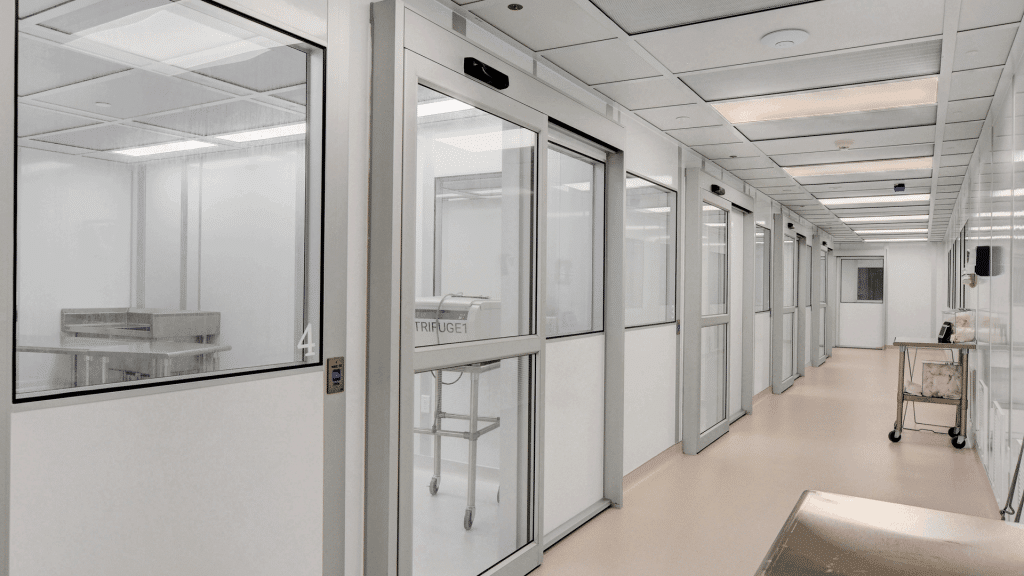
Contact
Leave Your Cleanroom in Expert Hands
FAQs About Semiconductor Cleanrooms
What ISO classes are typical for fabs and metrology?
ISO 4-5 for core fabs; ISO 6-7 for metrology.
Why are amber lights in semiconductor cleanrooms?
They block blue/UV light, protecting photoresist integrity.
What’s the difference between HEPA filters and ULPA filters?
ULPA filters trap 99.999% at 0.12µm; HEPA filters capture 99.97% at 0.3µm. ULPA is preferred for submicron nodes.
Why do these spaces use raised floors?
Raised floors let air return evenly and reduce ESD, cutting turbulence around 30%.
Why do fabs control HVAC to ±1°F and ±5% RH?
Redundant zones and sensors stabilize conditions, eliminating drift-related defects.
Why is redundant HVAC important in semiconductor cleanrooms?
It guarantees 100% uptime, saving $50K per hour of avoided downtime.


